

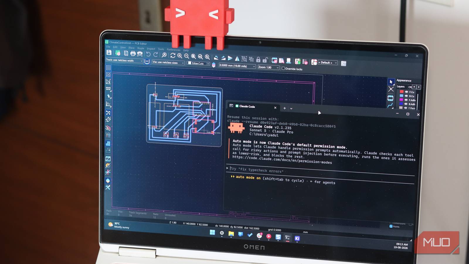

PCB design with Claude is now practical, not theoretical. An open-source bridge called KiCad-MCP connects Claude directly to KiCad’s PCBnew API. Describe the circuit in plain English. Claude writes the Python code that drives KiCad. The board appears on screen. Iterate by talking. That’s it.
Testing PCB design with Claude using zero recent KiCad experience — my last board was a college project fifteen years ago — produced a working ESP32 sensor board in forty-five minutes. The Gerbers checked out on the first try.
Let me show the exact setup for your first board.
Why PCB Design Was Always Hard
Traditional PCB design forces CAD-tool thinking. Components placed by coordinates. Traces routed by hand, nudged millimeter by millimeter. Symbol libraries, footprint libraries, 3D model libraries managed separately — each with unique quirks and naming conventions.
The schematic editor demands knowing the difference between a net label and a global label. The layout editor punishes missing design rules before routing starts. The footprint wizard is its own nightmare.
Most beginners quit at “associate footprints.” Happened to me twice.
Complexity isn’t the problem. The tools expose every knob and lever simultaneously, with zero guardrails. You’re not designing a circuit. You’re managing a database of geometric constraints.
Enter KiCad-MCP: The Bridge That Changes Everything
KiCad-MCP is an open-source Model Context Protocol server sitting between Claude and KiCad. It exposes KiCad’s Python API as tools Claude can call. Say “add a 10k resistor to the schematic.” Claude calls the MCP tool. The resistor appears.
The project lives on GitHub (kicad-mcp/kicad-mcp). Free, open source, actively maintained. Clean architecture: TypeScript MCP server handles protocol, modular Python backend does board manipulation.
Understanding MCP isn’t required. Installation is.
What You Need Before Starting
Hardware and software requirements:
– KiCad 8.0 or newer (free from kicad.org)
– Claude Desktop app with Pro or Max subscription (free web version can’t run MCP servers)
– Git and Node.js installed (for building the MCP server)
– A GitHub account (to clone the repo)
Mental prerequisites:
– Basic electronics knowledge (resistor, capacitor, microcontroller functions)
– Willingness to read error messages and retry
– Patience — bleeding-edge stuff breaks
That’s the list. KiCad’s interface stays unknown. Python skills stay unnecessary. PCB design with Claude handles the code for you.
Step 1: Install KiCad-MCP Server
Open your terminal. Clone the repository:
git clone https://github.com/kicad-mcp/kicad-mcp.git
cd kicad-mcp
Install dependencies and build:
npm install
npm run build
Compilation takes thirty seconds. “Build complete” without red errors means you’re ready.
Step 2: Configure Claude Desktop
This step traps most people. Claude Desktop reads MCP configuration from a JSON file. Location depends on OS:
macOS: ~/Library/Application Support/Claude/claude_desktop_config.json
Windows: %APPDATA%\Claude\claude_desktop_config.json
Linux: ~/.config/Claude/claude_desktop_config.json
Create the file if missing. Add this configuration:
{
  "mcpServers": {
    "kicad": {
      "command": "node",
      "args": ["/full/path/to/kicad-mcp/dist/index.js"],
      "env": {
        "KICAD_PYTHON_PATH": "/Applications/KiCad/KiCad.app/Contents/Frameworks/Python.framework/Versions/Current/bin/python3"
      }
    }
  }
}
Replace /full/path/to/kicad-mcp with your actual clone path. The KICAD_PYTHON_PATH must point to KiCad’s embedded Python — critical detail. Windows typically uses C:\Program Files\KiCad\8.0\bin\python.exe. Linux typically uses /usr/bin/python3.
Restart Claude Desktop completely. Quit and reopen. A small hammer icon in the chat input’s bottom-left corner confirms MCP connection.
Step 3: Create Your First Schematic with AI
Start a new chat in Claude. Say this exactly:
“I want to design a simple PCB. Create a new KiCad project called ‘esp32-temp-sensor’ in my Documents folder. Then add an ESP32-DevKitC-V4, a DS18B20 temperature sensor, a 4.7k pull-up resistor, and a 0.1µF decoupling capacitor. Connect the sensor data pin to GPIO 4, the resistor between data and 3.3V, and the capacitor across the sensor’s power pins.”
Watch what happens. Claude will:
1. Create the project and schematic file
2. Search symbol libraries for each component
3. Place them on the schematic canvas
4. Wire connections using net labels
5. Annotate reference designators (U1, R1, C1, etc.)
The schematic appears in KiCad’s window in real time. Weirdly satisfying.
Pro tip: Missing symbol? Claude tells you. Say “use a generic 8-pin MCU symbol for the ESP32” or “create a custom symbol for the DS18B20.” Both work.
Step 4: Lay Out the Board Without Headaches
Now the fun part. Say:
“Switch to the PCB editor. Set the board outline to a rounded rectangle, 60mm by 40mm, with 2mm corner radius. Place the ESP32 module near the left edge, USB connector facing out. Put the sensor near the right edge. Route traces with 0.2mm width, 0.2mm clearance. Add a ground pour on both layers.”
Claude will:
1. Create the board outline
2. Place components with reasonable orientation
3. Run the auto-router (or manual routing via API calls)
4. Add copper pours connected to GND net
5. Generate 3D view
Iterate freely: “Move the sensor closer to the edge.” “Make the USB connector overhang by 2mm.” “Add mounting holes at four corners, 3mm diameter.”
Each instruction triggers a new API call. The board updates live.
Step 5: Export for Manufacturing
Once satisfied, say:
“Generate Gerber files and drill files for JLCPCB. Use the standard 2-layer stackup. Include the edge cuts layer. Zip everything up.”
Claude runs plot and drill commands, packages files, tells you the location. Upload to JLCPCB, PCBWay, or preferred fab. Five boards cost $2.
Two weeks later, solder components. It works.
Pro Tips for Better Results
Use version control. Initialize a git repo in your project folder. Commit after each major step. Claude makes mistakes — sometimes deletes traces it just routed. Git rolls back instantly.
Be specific about constraints. “Route with 0.2mm traces” beats “route the board.” “Keep the antenna area clear” prevents non-functional WiFi boards.
Use the 3D view. “Show me the 3D render” after placement catches mechanical conflicts (USB connector hitting enclosure, tall components blocking each other) before fabrication.
Save your prompts. Working prompts become a personal PCB design library. Next board takes ten minutes.
Don’t trust everything. Always run KiCad’s DRC (Design Rule Check) before exporting. Claude misses things — unconnected nets, overlapping courtyards, missing keepout zones. DRC catches them.
Takeaway: Your First PCB Is One Conversation Away
PCB design used to demand months of learning. Now it’s an afternoon conversation. The tools haven’t changed — KiCad remains KiCad. The interface has. Talk. Code executes. Boards appear.
Start simple. Blinky LED board. Sensor breakout. Power supply module. Each teaches vocabulary for the next.
When weird errors hit — “footprint not found,” “net class not defined,” “zone fill failed” — paste the error into Claude. It fixes them. That’s the real superpower: not designing boards, but debugging them together.
Go make something. The fab house is waiting.